As semiconductor manufacturing scales past the 3nm threshold into sub-2nm Gate-All-Around (GAA) nanosheet transistors and 3D NAND architectures surpassing 300 layers, electrical power delivery within cleanroom processing equipment has transitioned from a supporting utility to a primary determinant of wafer die yield. Modern semiconductor toolsets—including Plasma-Enhanced Chemical Vapor Deposition (PECVD), Atomic Layer Deposition (ALD), Reactive Ion Etching (RIE), Ion Implantation, and EUV light source power modules—demand an unprecedented level of voltage stability, current response speed, and spectral purity.

In semiconductor plasma processing, minor variations in bias voltage or current ripple can destabilize the plasma sheath, altering ion energy distribution functions (IEDF). This instability induces critical dimension (CD) drift, localized micro-trenching, line-edge roughness (LER), and gate oxide breakdown. Furthermore, in high-aspect-ratio (HAR) contact etch processes, parasitic micro-arcs occurring within the plasma chamber present an immediate threat of wafer burn-off, resulting in scrap costs exceeding tens of thousands of dollars per silicon substrate.
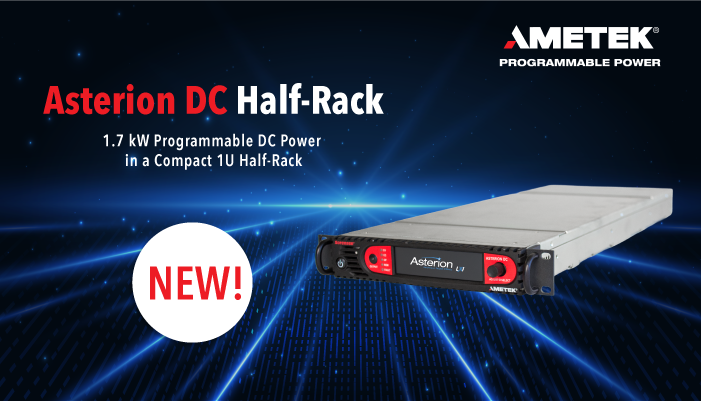
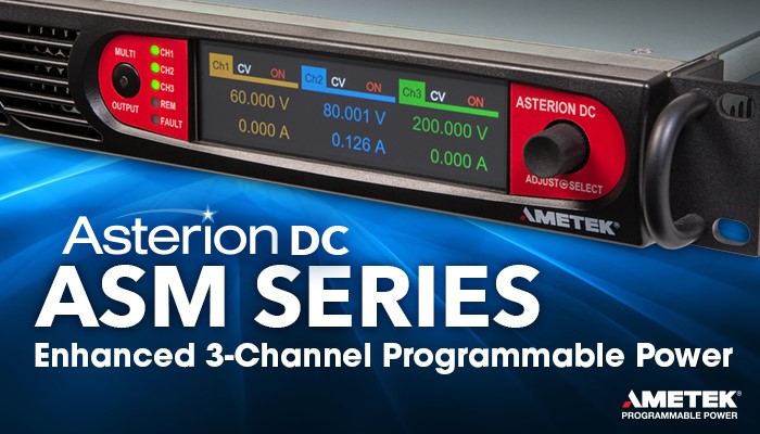
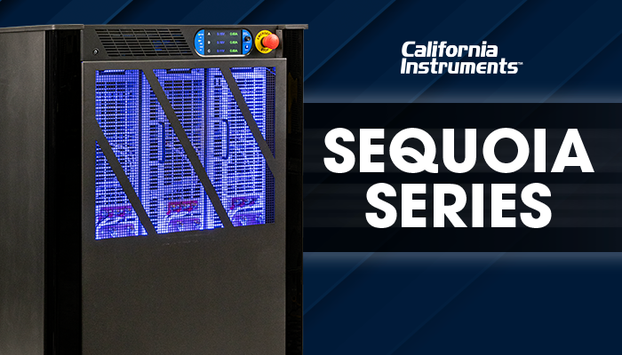
AMETEK Programmable Power addresses these severe fab challenges through purpose-built semiconductor manufacturing power supplies. Combining legacy expertise from Sorensen, California Instruments, and Elgar brands, our modular AC and DC power instruments supply low-noise, highly reliable power tailored for cleanroom OEM tool integrators and fab yield enhancement directors.
Core Electrical Parameters Required in Wafer Processing Equipment
Selecting programmable AC/DC power supplies for wafer fab tools requires evaluating critical domain-specific parameters that dictate long-term process repeatability and machine uptime:
- Ultra-Low Ripple & Noise (<0.05% RMS): Essential for preventing electric field fluctuations in electrostatic chuck (ESC) clamping forces and maintaining precise plasma sheath potentials.
- Microsecond Arc Energy Management (<1 µs Response): Ultra-fast hardware shutoff circuits limit thermal damage during unexpected chamber arcing by quenching arc energy before micro-structural defects occur on the wafer surface.
- SEMI F47 Voltage Sag Immunity: Guarantees continuous power delivery during utility grid sags and transients, keeping critical vacuum pumps, wafer handlers, and RF generators operational without tool faulting.
- High Channel Isolation (Up to 1500V DC): Eliminates ground loops and electromagnetic interference (EMI) crosstalk across multi-chamber tools with multi-rail bias and heater loads.
Senior SEO Director & Power Systems Architect Insight
"In 300mm sub-2nm wafer manufacturing, total cost of ownership (TCO) is directly proportional to mean time between failures (MTBF) and zero-scrap yield consistency. Standard industrial power supplies lack the microsecond arc quenching, tight load regulation under rapid plasma ignition transients, and SEMI F47 compliance needed for fab tool certification. Integrating cleanroom-tested, autoranging programmable power supplies ensures process repeatability across global multi-fab deployments."